
New Delhi, March 17: Amid ongoing tensions in West Asia and rising concerns over energy supply, India's Ministry of Petroleum and Natural Gas has outlined a series of measures to accelerate the adoption of Piped Natural Gas (PNG) and expand city gas infrastructure across the country.
As part of the push, the government has encouraged consumers, particularly commercial LPG users in major cities and urban areas, to switch to PNG.
City Gas Distribution (CGD) companies have also been advised to proactively approach potential customers and facilitate connections through multiple channels, including email, customer portals, letters, and call centres.
The ministry noted that several CGD entities are offering incentives to boost PNG adoption, as authorities seek to reduce dependence on conventional LPG supplies during a period of global uncertainty.
In a communication on Monday, the Centre has requested state governments and Union Territories to expedite approvals and remove procedural bottlenecks for laying CGD pipelines.
The measures highlighted include granting deemed permissions for pending applications related to pipeline infrastructure; ensuring approval of new CGD permissions within 24 hours; waiving road restoration and other permission charges levied by state or local authorities; relaxing working hours and seasonal restrictions to accelerate project execution; and appointing state-level nodal officers to strengthen coordination and enable faster implementation
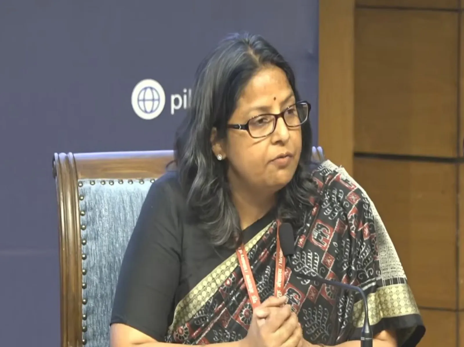
Sujata Sharma, Joint Secretary, Ministry of Petroleum and Natural Gas, addressing an inter-ministerial press briefing on Tuesday that there is adequate crude oil inventory in the country, but LPG supply continues to remain a bit concern.
"Petrol and diesel are available in sufficient quantity. Regarding natural gas, as I told you, the Government of India is making efforts and it would be beneficial if all commercial LPG consumers shifted to PNG...," she said.
Despite concerns around LPG supply, there have been no reports of dry-outs of gas supply at LPG distributorships across India, Sujata Sharma said.
Similarly, no cases of fuel dry-outs have been reported at retail outlets by Oil Marketing Companies, and supplies of petrol and diesel continue to be maintained regularly. However, citizens are advised not to resort to panic buying as adequate stocks of petrol and diesel are available across the country.
State Governments are undertaking enforcement measures to prevent hoarding and black marketing of petrol, diesel and LPG. Raids are being carried out in several states to check hoarding and black marketing of LPG cylinders.
"Regarding enforcement action, so far, about twelve thousand raids have been conducted in the last few days. About fifteen thousand cylinders have been seized...Yesterday in Delhi, about six hundred cylinders were seized. Similarly, in Uttar Pradesh, about four hundred and fifty inspections and raids have been conducted in the last few days. Ten people have also been arrested. In Jammu and Kashmir, five hundred and sixty-four raids have been conducted, FIRs have been filed, and arrests have also been made. In Kerala, about a thousand raids and inspections have been conducted and domestic and commercial cylinders have been seized. In Madhya Pradesh, too, about twelve hundred raids have been conducted and about eighteen hundred cylinders have been seized. Apart from this, the inspection teams of our oil marketing companies have also been activated and surprise inspections have been conducted at about two and a half thousand retail outlets and LPG distributorships...," Sujata Sharma said.
Alternate fuels such as kerosene and coal have been activated for certain sectors, including hospitality and restaurants, to ease pressure on LPG supplies.
At the inter-ministerial briefing, Rajesh Kumar Sinha, Shipping Ministry, GoI said all Indian sailors and ships are safe in the Gulf region.
In the last 24 hours, 161 Indian sailors have been repatriated and brought back to India.
"This work was done in coordination with our embassies and missions. The second LPG carrier, Nanda Devi, reached Kandla at around 2:30 am today, and now cargo is being discharged from both the LPG carriers, Shivalik and Nanda Devi. There are multiple discharges. The discharge of Nanda Devi is ship-to-ship, from mother ship to daughter ship. It is currently underway. All efforts have been made to streamline vessel movement and cargo operations at the port."
On media reports this morning that around 450 containers are lying on the road at Jawaharlal Nehru Port, he rubbished them as "baseless".
"The containers are in the CFS, Container Freight Stations, in the warehouse and in the factory premises, which is as per the policy of JNPA...," he asserted. (ANI)